Matrix Hexpansion base v2 (lite)
A versatile hexpansion breakout and co-processor board for prototyping or controlling many LEDs very cheaply.
The matrix output pins (and GPIO, data, and power pins in v2) are brought out as large through-hole pads with 2.54mm spacing. This allows a second, much cheaper, board to be grafted onto this one. I hope this lowers the bar of entry to making (LED matrix or not!) hexpansion boards: those secondary boards do not require the expensive ENIG surface, or necessarily the soldering of tiny SMD parts.
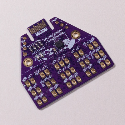
BOM
Examples
Source files, pinout, and making a daughter board
Find the schematic and KiCad project for this board on Github.
A daughter board for the matrix hexpansion does not need to be expensive: five copies of a typical board can be procured from regular PCB houses for about £5 (shipped, but not assembled). Unlike a regular hexpansion PCB, this does not need an edge connector or the more expensive ENIG coating. Of course, you still have to assemble it with your choice of size and count of LEDs (or pay for PCBA).
It must have space for the parent board footprint to be placed. The SMD version has pads on the bottom of the daughter board only and but may require a hot air rework tool and solder paste for assembly; there also is a through hole version for assembly with a regular soldering iron, the latter is also compatible with standard 2.54mm pin header spacing.
Example schematics for the charlieplexed wiring are provided for two different matrix layout options. The lite-loop example board can drive 156 LEDs using 13 column pins (with reduced brightness and refresh rate). The second (not finished yet) has 60 or 72 LEDs, in two independent matrices of six or seven column pins each (where two columns can be active at once, so the LEDs can be brighter).
One resistor per GPIO pin is required. Ideally, all LEDs should be the same colour to get more or less uniform brightness across the matrix. With the second example two colours can be used with different resistors on each set of column pins. However, brightness will also slightly reduce as more LEDs per column are active because the output voltage on the GPIO pins drops with higher current draw.
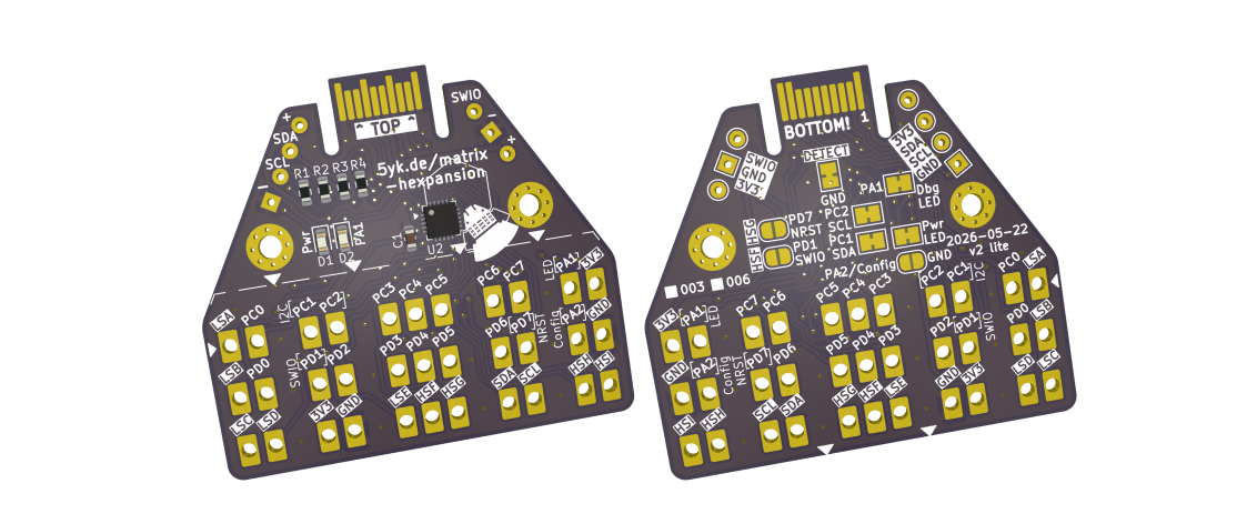
Pinout
There are three rows of 13 rectangular pads with 2.54mm spacing and 1.5mm round holes; the holes are larger than usual to facilitate soldering from the bottom side to another PCB to be placed on top of this one. Silkscreen labels mark the purpose of each pad, with the inverted labels indicating pins from the hexpansion connector, and the other pins being directly connected to the co-processor GPIO pins. Pins marked with square brackets or stars may have a special use precluding them from being used for general purpose IO.
| LS1 | PC0 | PC1 (SDA) | PC2 (SCL) | PC3 | PC4 | PC5 | PC6 | PC7 | PA1 (LED) | 3V3 | ||||
| LS2 | PD0 | PD1 (SWDIO) | PD2 | PD3 | PD4 | PD5 | PD6 | PD7 (NRST) | PA2 (Config) | GND | ||||
| LS3 | LS4 | 3V3 | GND | LS5 | HS1* | HS2* | SDA | SCL | HS3 | HS4 |
The first two rows contain all the GPIO and power pins for the co-processor and two low-speed badge pins. The third row, and perhaps even the two outer columns can be excluded for making very small LED boards. This requires about 40×10mm of space at the top edge of the daughter board.
The third row has the remaining badge pins (four further low-speed GPIOs, all four high-speed GPIOs, power, and the I2C data and clock lines). It is intended for more general prototyping and can be used even if this board is not populated with a co-processor.
Special pins
There are some GPIO pins that can not be used as matrix outputs, leaving 13 that can (including PD7 unless used for badge interrupts). There are solder jumpers on the back of the board for these where it may make sense to disconnect them from their special use.
- The PC1 and PC2 I2C data and clock pins are connected via jumpers to the hexpansion connector and pull-up resistors R3 and R4. Remove the jumpers if you do not want the processor to communicate with the badge.
- PD1 is the SWIO programming pin and cannot be used as a GPIO; optionally this can also be connected to HS2 (unlikely to be useful, unless you want to try your hand at making the badge into something like the esp32-s2-funprog).
- PD7 is the reset pin but usually configured as a GPIO via user option bytes. By default it is connected to HS1 and used to enter the bootloader after a power cycle. It can still be used to drive LEDs in the main program, but should not be pulled low or high by the daughter board during boot.
- PA1 drives the on-board LED D2; break the jumper to use if for something else.
- PA2 can be pulled to GND with a solder jumper and should be set as an input with internal pull-up if used for assembly-time configuration.
Boards with a version before v2.1 labelled the HS and LS pins with letters (LSA-LSE, HSF-HSG); this has been changed to numbers (LS1-LS5, HS1-HS4) to match the hexpansion interface documentation, but the layout is the same. They also had slightly different default jumper configurations; it is now no longer necessary to close the PD7 jumper to enable firmware updates from the badge.